

HD31217 RF Amplifier
Module
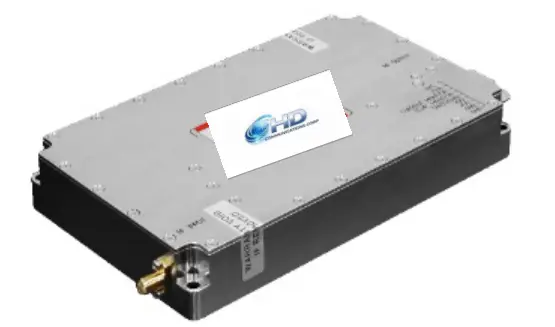
HD31217
| FREQUENCY RANGE1–1,000 MHz | GAIN44 dB minimum |
| SATURATED OUTPUT · CW25 W minimum | OUTPUT AT P1 dB · CW12 W minimum |
| DC SUPPLY28–30 VDC | CONFIGURATIONClass A/AB module |
HD31217 electrical specifications
| Parameter | Specification | Conditions / notes |
|---|---|---|
| Operating frequency range | 1–1,000 MHz | Instantaneous bandwidth |
| Output power at Psat | 25 W minimum | CW |
| Output power at P1 dB | 12 W minimum | CW |
| Power gain | 44 dB minimum | 0 dBm or less input for rated output |
| Power gain flatness | 3 dB peak-to-peak maximum | Constant input power |
| Input return loss | −10 dB maximum | Designation as printed in the datasheet |
| Two-tone intermodulation (IMD) | −30 dBc typical | 34 dBm per tone; tone spacing Δ = 1 MHz |
| Second harmonic | −20 dBc typical | At rated output power |
| Third harmonic | −12 dBc typical | At rated output power |
| Spurious output | −60 dBc maximum | Non-harmonics |
| Operating voltage | 28–30 VDC | DC supply |
| Current consumption | 5 A maximum / <4 A typical | At rated output power |
| Input-power protection | +8 dBm maximum | Less than 10 seconds without damage |
| Load-VSWR protection | ∞:1 | Less than 1 minute at rated output power |
9-pin D-Sub interface
| Pin | Function | Description |
|---|---|---|
| 1 | FWD | Forward monitoring — option 101 |
| 2 | REV | Reverse monitoring — option 102 |
| 3 | Current sensor | ID: 50 mV / 100 mA typical |
| 4 | Temperature sensor | VT: 10 mV/°C + 500 mV typical |
| 5 | Shutdown (open collector) | Enable: TTL high or open. Disable: TTL low or short. |
| 6, 7 | VDD | 28 VDC, as labeled in the pin-assignment table |
| 8, 9 | GND | Ground |
The electrical table specifies a 28–30 VDC operating range; the pin table labels VDD as 28 VDC. Forward and reverse monitoring are optional. Confirm the selected options and connector orientation against the delivered documentation before wiring.
Operating and storage conditions
| Operating case temperature | −20 to +75°C |
|---|---|
| Storage temperature | −40 to +85°C |
| Relative humidity | Up to 95%, non-condensing |
| Altitude | 3,000 m |
| Shock and vibration | Normal transport |
Military specifications are available for quotation according to the datasheet. They are not stated as standard qualifications for every HD31217 module. Include any required environmental or qualification standard in your inquiry.
Documentation for design-in
About HD31217
HD31217 covers 1–1,000 MHz (1 MHz–1 GHz) with instantaneous bandwidth. The datasheet’s electrical specifications are given at 50 Ω and 25°C.
The 25 W minimum rating is saturated output (Psat), CW. Output at the 1 dB compression point (P1 dB) is 12 W minimum, CW. Choose the operating level around the distortion and signal-peak requirements of your application.
The operating range is 28–30 VDC, with 5 A maximum and less than 4 A typical current consumption at rated output. An external heatsink with forced-air cooling is required. Keep operating case temperature within −20 to +75°C.
HD31217 is an amplifier module for installation in host equipment. It uses SMA female RF connectors and a 9-pin D-Sub interface. The host design must provide DC power, mounting and cooling.
The D-Sub interface provides current sensing, temperature sensing and open-collector shutdown control. Pin 5 enables the amplifier when TTL high or open, and disables it when TTL low or short. Forward monitoring (option 101) and reverse monitoring (option 102) are optional.
The datasheet specifies +8 dBm maximum input for less than 10 seconds without damage, and ∞:1 load VSWR for less than 1 minute at rated output. These time limits do not permit continuous overdrive or mismatch.
Open HD31217 V2.2.pdf directly. Page 1 contains specifications and pin assignments; page 2 contains the mechanical outline drawing.
Include quantity, operating frequencies, required Psat or P1 dB output, waveform, signal bandwidth, distortion target and integration constraints. Note whether you need forward or reverse monitoring, qualification requirements and your delivery target.