

HD31261 RF Amplifier
Module
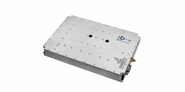
HD31261
| FREQUENCY RANGE800–4,200 MHz | SATURATED OUTPUT (PSAT)100 W minimum CW |
| POWER GAIN50 dB minimum | SUPPLY VOLTAGE32 VDC nominal |
| CONFIGURATIONModule | CATEGORYLow Frequency Amplifier Module |
HD31261 electrical specifications
From the matching HD31261 V1.2 datasheet. Test conditions: 50 Ω, 25 °C. Minimum, maximum and typical ratings retain the datasheet qualifiers.
| Parameter | Specification | Conditions / notes |
|---|---|---|
| Operating frequency | 0.8–4.2 GHz | — |
| Saturated output (Psat) | 100 W minimum | CW; 0.3 dB lower at 4.0–4.2 GHz |
| Output at P1 dB | 40 W minimum | CW |
| Power gain | 50 dB minimum | 0 dBm or less for rated output |
| Gain flatness | 3.0 dB p-p maximum | Constant input power |
| Input return loss | −10 dB maximum | Relative to 50 Ω |
| Two-tone IMD | −30 dBc typical | 40 dBm/tone; Δ = 1 MHz |
| Harmonics | 2nd −15 dBc; 3rd −20 dBc, typical | At rated output |
| Spurious | −60 dBc maximum | Non-harmonic |
| Operating voltage | 32 VDC nominal | — |
| Current consumption | 16 A maximum | At rated output |
| Input power protection | +8 dBm maximum | Less than 10 seconds without damage |
| Load VSWR protection | 5:1 maximum | Less than 1 minute at rated output |
HD31261 interface and pin assignments
Pin assignments from the matching HD31261 datasheet. Optional signals are identified separately from standard connections.
| Pin | Function | Description |
|---|---|---|
| 1 | N/C | No connection |
| 2 | VVA | Option 103 |
| 3 | Current sensor | 20 mV / 100 mA typical |
| 4 | Temperature sensor | 10 mV/°C + 500 mV typical |
| 5 | Shutdown | Enable: TTL high or open; disable: TTL low or short |
| A1 | VDD | 32 VDC |
| A2 | GND | Ground |
HD31261 operating and storage conditions
Environmental limits from the matching model datasheet.
| Parameter | Specification | Conditions / notes |
|---|---|---|
| Operating case temperature | −20 to +75 °C | — |
| Storage temperature | −40 to +85 °C | — |
| Relative humidity | Up to 95% | Non-condensing |
HD31261 mechanical specifications and cooling
Use the model-specific outline drawing in the PDF when planning mounting and connector clearance.
| Parameter | Specification | Conditions / notes |
|---|---|---|
| Dimensions | 220 × 144 × 27 mm | Excluding connectors |
| Weight | 1.7 kg | — |
| RF input / output | SMA female | — |
| Power / interface connector | 7-pin hybrid D-Sub, 7W2 | — |
| Cooling | External heatsink | Forced air required |
HD31261 documentation
The linked file is HD31261 V1.2.pdf, matched to HD31261. It contains electrical, environmental and mechanical specifications, pin assignments and outline drawings. Check the drawings for the selected options; specifications and drawings may vary with options.
About HD31261
The HD31261 datasheet lists 0.8–4.2 GHz.
Saturated output (Psat): 100 W minimum; CW; 0.3 dB lower at 4.0–4.2 GHz. Output at P1dB: 40 W minimum; CW.
32 VDC nominal. Current consumption: 16 A maximum; at rated output.
Pin 1: N/C — No connection. Pin 2: VVA — Option 103. Pin 3: Current sensor — 20 mV / 100 mA typical. Pin 4: Temperature sensor — 10 mV/°C + 500 mV typical. Pin 5: Shutdown — Enable: TTL high or open; disable: TTL low or short. Pin A1: VDD — 32 VDC. Pin A2: GND — Ground.
External heatsink; Forced air required. Operating case temperature: −20 to +75 °C. Storage temperature: −40 to +85 °C.
Input power protection: +8 dBm maximum; less than 10 seconds without damage. Load VSWR protection: 5:1 maximum; less than 1 minute at rated output.
Open HD31261 V1.2.pdf for the complete ratings, pin assignments or control options, and outline drawings.
Request a quote for HD31261
Source-checked power ratings
100 W minimum CW Psat (0.3 dB lower at 4.0–4.2 GHz); 40 W minimum CW P1dB
50 ohms, 25°C. Psat is 0.3 dB lower at 4.0–4.2 GHz in CW.
Datasheet V1.2 — page 1